
The continuous increase in clock frequencies has made phase noise and jitter increasingly important factors in system timing. This article discusses their concepts and impact on system performance, and provides effective methods for reducing phase noise and jitter at the circuit board level, chip level, and module level.
Under this trend, designers of high-speed digital devices are paying more attention to timing factors. This article introduces the fundamental concepts of phase noise and jitter, analyzes their impact on system performance, and presents commonly used circuit techniques that can minimize phase jitter and noise.
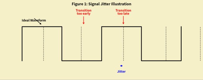
Figure 1: Signal Jitter Illustration
What are Phase Noise and Jitter?
Phase noise and jitter are two different quantitative representations of the same phenomenon. Ideally, the duration of a perfect pulse signal at a fixed frequency (e.g., 1 MHz) should be exactly 1 microsecond, with a transition edge every 500 ns.
However, such a signal does not exist in practice. As shown in Figure 1, the length of the signal period always varies to some extent, causing the arrival time of the next edge to be uncertain. This uncertainty is phase noise, or jitter.
Jitter is a Time-Domain Concept
Jitter is a measurement of signal variation in the time domain. It essentially describes how much the signal period deviates from its ideal value. Typically, period variations in signals below 10 MHz are not classified as jitter, but rather as offset or drift. There are two main types of jitter: deterministic jitter and random jitter.
Deterministic jitter is caused by identifiable interference signals. It usually has a limited amplitude, a specific (non-random) cause, and cannot be analyzed statistically. The four main sources of deterministic jitter are:
1. Crosstalk between adjacent signal traces: When the self-inductance of a conductor increases, it converts the induced magnetic field around adjacent signal lines into induced current, which increases or decreases the voltage, thereby causing jitter.
2. EMI radiation on sensitive signal paths: Power supplies, AC power lines, and RF signal sources are all EMI sources. Similar to crosstalk, when EMI radiation is present nearby, noise currents induced on the timing signal path will modulate the voltage value of the timing signal.
3. Noise on the power plane in multi-layer substrates: This noise can change the threshold voltage of logic gates or alter the reference ground level of the threshold voltage, thereby changing the voltage required to switch the gate circuit.
4. Multiple gate circuits switching to the same logic state simultaneously: This can cause spike currents to be induced on the power plane and ground plane, which may cause the threshold voltage to change.
Random jitter refers to timing variations caused by factors that are difficult to predict. For example, temperature factors that can affect the mobility of semiconductor crystal materials may cause random variations in carrier flow. Additionally, variations in semiconductor manufacturing processes, such as non-uniform doping density, can also cause jitter.
The most fundamental characteristic of random jitter is its randomness, so we can use a Gaussian statistical distribution to describe its properties. For example, if we take 100 consecutive measurements of the oscillation period of a clock oscillator that contains only random jitter factors, the results will follow a Gaussian distribution (also called a normal distribution). Within one standard deviation from the mean, 68.26% of all period measurements are contained; within ±2 standard deviations, 95.4%; within ±3 standard deviations, 99.73%; and within ±4 standard deviations, 99.99366%.
From this normal distribution, we can derive two common jitter definitions:
1. Peak-to-peak jitter: the difference between the minimum and maximum measured values on the normal curve. In most circuits, this value increases with the number of measurement samples and theoretically can reach infinity. Therefore, this measurement is of limited significance.
2. RMS (Root Mean Square) jitter: the value of the first standard deviation of the normal distribution. This value does not change significantly with an increase in the number of samples, making this measurement more meaningful. However, this measurement is only valid for pure Gaussian distributions. If any deterministic jitter exists in the distribution, using the first-order variance of the entire jitter histogram to estimate the probability of jitter occurrence would be incorrect.
3. Multiple random jitter sources can be added in an RMS manner. However, to obtain the total jitter, the peak-to-peak value must be used so that random jitter can be added to deterministic jitter.
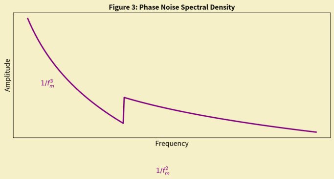
Figure 3: Phase Noise Spectral Density
Phase Noise is a Frequency-Domain Concept
Phase noise is another way of measuring signal timing variations, with results displayed in the frequency domain. Figure 2 uses an oscillator signal to explain phase noise.
If there were no phase noise, all the power of the oscillator would be concentrated at frequency f = f₀. However, the presence of phase noise spreads a portion of the oscillator's power into adjacent frequencies, generating sidebands. As shown in Figure 2, at a reasonable distance from the center frequency, the sideband power rolls off at 1/fₘ, where fₘ is the frequency offset from the center frequency.
Phase noise is typically defined as the dBc/Hz value at a given offset frequency, where dBc is the ratio (in dB) of the power at that frequency to the total power. The phase noise of an oscillator at a certain offset frequency is defined as the ratio of the signal power within a 1 Hz bandwidth at that frequency to the total power of the signal.
In Figure 2, phase noise is represented by the ratio of the area of the rectangle within a 1 Hz bandwidth at the offset frequency f to the area under the entire power spectrum curve, which is approximately equal to the difference between the curve height at the center frequency and the curve height at fₘ. This curve shows the power spectrum of an oscillator with noisy phase angles, and the fluctuations of these noise phase angles themselves are shown in Figure 3.
Figure 2 shows the power spectrum of the oscillator, while Figure 3 shows the spectrum of the noise phase angles, also called the spectral density of phase fluctuations. For offset frequencies sufficiently far from the center frequency, the phase noise measured in dBc/Hz from the power spectrum in Figure 2 equals the value of the phase fluctuation spectral density at that frequency shown in Figure 3.
The density spectrum in Figure 3 is displayed on a logarithmic scale, where the phase noise sidebands decrease at a rate of 1/fₘ² or 20 dB/decade. In practice, in certain regions of the noise sidebands, the phase noise may decrease at rates of 1/f³, 1/f², or even 1/f⁰, depending on the relevant noise processes.
The region with a 1/f² decrease rate is called the "white frequency" fluctuation region, where phase variations are caused by white or uncorrelated fluctuations within the oscillator period. The behavior of the oscillator in this region is determined by the thermal noise of the components in the oscillator circuit. When the offset frequency is sufficiently low, the flicker noise of the components also comes into play, causing the spectral density in this region to decrease at a rate of 1/f³.
It is also worth noting that as the offset frequency in Figure 3 approaches 0, the sideband noise approaches infinity. This is consistent with the timing jitter behavior expected in a free-running oscillator.
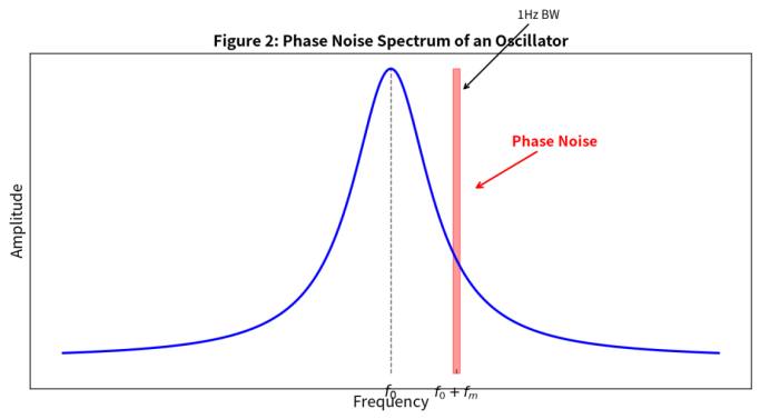
Figure 2: Phase Noise Spectrum of an Oscillator
How to Convert Phase Noise to Jitter
Jitter and phase noise describe the characteristics of the same phenomenon, so it is meaningful to derive the jitter value from phase noise measurement results. The following describes the derivation method: each oscillator has its phase noise plot. Figure 4 is an example showing the phase noise of an oscillator in the frequency range from 12 kHz to 10 MHz. In the figure, L(f) gives the distribution of sideband noise in the form of a power spectral density function, in units of dBc. The power at the center frequency is not important because jitter only reflects the relative power of phase noise (i.e., modulation) to the "pure" center frequency. The total noise power in the sidebands can be obtained by integrating the L(f) function over the frequency band of interest (12 kHz to 10 MHz).
This yields the power of phase modulation noise in that frequency band, and phase modulation is what causes jitter. From this, we can derive the RMS jitter value using the following definite integral.
The following equation can be used to calculate the RMS jitter caused by this noise power:
N = Noise Power = ∫ ℒ(f) df (from 12 kHz to 20 MHz)
(1)
The jitter value can also be expressed in other units, such as unit intervals (UI) or time. Dividing the above equation by the center frequency in radians converts the jitter unit to time, as shown in the following equation:
RMS Phase Jitter (radians) = √(10^(N/10)) × 2
(2)
Using the noise power values plotted in Figure 4, we can calculate the RMS jitter of a 312.5 MHz oscillator. Integrating the phase noise curve from 12 kHz to 20 MHz yields −63 dBc:
Integration curve = ∫ ℒ(f) df (from 12 kHz to 20 MHz) = −63 dBc
(4)
Therefore, the RMS phase jitter value in radians can be obtained as follows:
RMS Jitter = √(10^(−63/10)) × 2 = 1415×10⁻⁶ radians
(5)
The jitter value can also be converted to picoseconds:
RMS Jitter (seconds) = Jitter (radians) / (2 × π × f_osc)
The typical total jitter value of the same 312.5 MHz oscillator is approximately 5 ps RMS.
RMS Jitter = 1415×10⁻⁶ / (2 × π × 312.5×10⁶) = 0.72 ps (rms)
(6)
Ultimately, the calculated RMS jitter value of 0.72 ps accounts for only a small proportion of the maximum jitter.
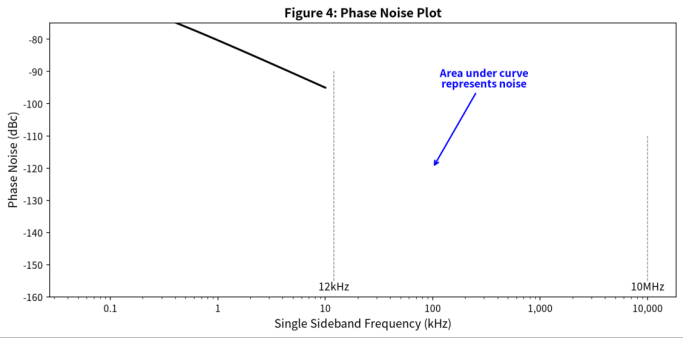
Figure 4: Phase Noise Plot
How to Minimize Phase Noise and Jitter on Circuit Boards
Circuit board designers can reduce deterministic signal jitter on the board through two key techniques:
1. Transmit and receive signals in differential form: Conventions such as LVDS or PECL, which transmit and receive signals in differential mode, can greatly reduce the impact of deterministic jitter. Furthermore, this differential path can eliminate all interference and crosstalk on the signal path. Since such signal transceiver systems inherently have high immunity to common-mode noise, the differential form itself has a tendency to eliminate jitter.
2. Careful routing: Avoid parasitic signals that could affect the signal path through crosstalk or interference. Traces should be as short as possible and should not cross traces carrying high-speed switching digital signals. If a differential signal transceiver system is adopted, the two differential signal traces should be as close together as possible to better utilize their inherent common-mode noise rejection characteristics.
How to Minimize Phase Noise and Jitter in Chips
At the chip level, the following design techniques can be used to minimize jitter:
1. Differential signal transceiving: Even if the signal entering the chip is single-ended, it is best to convert it to a differential signal within the chip, for the same reasons described in the previous section.
2. Careful routing of signal paths: When routing sensitive timing signal paths, caution must be exercised, and traces should be as short as possible, avoiding crossing any digital signal lines. Where conditions allow, it is best to display all these signal paths on the layout. For example, a signal path on the second metal layer can be sandwiched between the first and third metal layers, both of which are connected to a clean ground.
3. Proper buffer sizing: If buffers are used to distribute signals between modules, attention must be paid to the selection of drive strength. Insufficient drive will cause excessively slow signal rise/fall times, giving noise an opportunity to interfere.
4. Keep the substrate and ground clean: Substrate noise and ground noise are the main causes of deterministic jitter. Within a chip that has multiple synchronous digital outputs, ground bounce noise can reach several hundred millivolts, or even 1 volt. To reduce ground bounce noise, there should be as many power pairs as possible on the chip, and these power pairs should be placed as close as possible to the digital outputs.
5. Use a separate clean ground layer: In circuit design, it is best to separate the power supply of digital circuits from that of sensitive analog circuits (such as oscillators or PLLs). The power supply of digital circuits, especially high-drive-output digital circuits, is likely to introduce noise, and once this power supply is used for timing circuits, it will also become a major factor increasing jitter. Therefore, for circuits such as PLLs, power supply filtering can be used to further reduce the impact of power supply noise.
How to Minimize Phase Noise and Jitter in Unit Modules
The following techniques can be adopted when designing unit modules to reduce jitter:
1. Use tail current: There is a direct relationship between the current used in timing circuits and phase noise. For example, increasing the tail current of a differential pair will inevitably lead to improved jitter performance. Therefore, we must seek a balance between reducing jitter and reducing power consumption, selectively increasing the current of the most sensitive circuits where appropriate.
2. Careful layout: When laying out units that may cause phase noise, matched components (such as those connected to the inputs of a differential pair) should be oriented in the same direction and laid out as symmetrically as possible. This method ensures that matched components have the same process gradients, thereby helping to improve matching between components. Resistors should be as wide as possible to reduce the Delta-W effect. If possible, use the same type, and even the same size and resistance value, of resistors throughout the circuit to help track all variations in process and temperature.